Abstract
Solid State Drives (SSDs) utilize persistent NAND Flash Memory chips, completely eliminating mechanical platters and moving actuator arms. SSDs provide orders of magnitude faster random read/write access than traditional Hard Disk Drives. However, NAND flash introduces asymmetric operational constraints: memory can be programmed in small Pages but must be erased in large Blocks, requiring onboard Wear-Leveling algorithms to prevent cell degradation.
- Category: Non-Volatile Semiconductor Storage
- Core Architecture: Flash Translation Layer (FTL) over NAND chips.
- Key Constraint: Erase-before-write asymmetry and finite cell write endurance.
NAND Flash Architecture & Sizing Hierarchy
NAND flash chips are organized in a strict structural hierarchy:
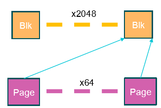
graph TD
    Chip["NAND Flash Chip"] --> Block["~2048 Erasable Blocks"]
    Block --> Page["~64 Programmable Pages (e.g., 2 KB - 4 KB per page)"]
    Page --> Cell["Floating-Gate / Charge-Trap Flash Cells"]
Asymmetric Read, Write, and Erase Rules
Unlike DRAM or magnetic storage, NAND flash cannot overwrite existing bits directly:
| Operation | Unit Granularity | Execution Constraints |
|---|---|---|
| Read | Page () | Fast (). Direct access by page index. |
| Program (Write) | Page () | Can only program pages whose bits have been completely erased (set to 1). |
| Erase | Block () | Slow (). Resets all cells in an entire block to 1. |
Flash Wear-Out & Wear-Leveling
Repeatedly erasing NAND flash blocks damages the insulating oxide layer of individual cells, leading to physical wear-out and bit degradation after a finite number of Program/Erase (P/E) cycles.
graph TD
    OS["OS Block Write Request"] --> FTL["Flash Translation Layer (FTL)"]
    FTL --> Check["Inspect Block Erase Counts"]
    Check --> Remap["Remap Logical Page to Least-Worn Physical Block"]
    Remap --> Write["Program NAND Page"]
To maximize drive lifespan, SSD controllers implement an internal microcontroller running a Flash Translation Layer (FTL):
- Wear-Leveling Algorithms: Distributes page writes uniformly across all physical blocks on the drive, ensuring no single block wears out prematurely.
- Garbage Collection: Consolidates valid pages from partially invalidated blocks into fresh blocks, enabling background block erasures.
- Out-of-Place Writes: Modifying an existing page writes the new data to an unused page elsewhere on the chip and marks the old physical page invalid.
HDD vs. SSD Architecture Comparison
| Attribute | Hard Disk Drives (HDD) | Solid State Drives (SSD) |
|---|---|---|
| Primary Technology | Magnetic platters & mechanical arms | Non-volatile NAND flash memory chips |
| Random I/O Latency | High ( seek/rotation) | Extremely Low () |
| Sequential Throughput | Moderate () | Extremely High () |
| Mechanical Reliability | Sensitive to physical drops and vibration | High physical durability (no moving parts) |
| Cost Per Bit | Low (economical for cold archival data) | Higher ( more expensive per GB) |
| Wear Degradation | No write-cycle limits on magnetic media | Finite P/E write cycles per flash cell |
OS File System Integration
Modern operating systems preserve the standard Block Interface for SSD compatibility. However, mechanical optimizations (such as track placement and elevator disk scheduling) are bypassed on flash media. New file systems incorporate explicit TRIM commands to inform the SSD controller when file blocks are deleted.