Abstract
Latches and Flip-Flops are bistable memory elements that form the foundation of sequential digital circuits. Unlike combinational circuits whose outputs depend solely on current inputs, sequential circuits utilize feedback loops to maintain internal state. A Latch is level-sensitive, continuously updating its output while its control/clock signal is active (transparent mode). A Flip-Flop is edge-triggered, sampling its input only during a specific clock transition (rising or falling edge) using a Master-Slave design. These primitives evolve from basic SR Latches to glitch-free D Flip-Flops with enable, reset, and preset capabilities.
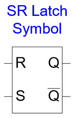
SR Latch (Set/Reset Latch)
An SR Latch is the simplest asynchronous bistable circuit built from two cross-coupled NOR or NAND gates.
Practical Application: Flight Attendant Call Button
- Press Call (): Light turns ON () and stays ON even after the button is released.
- Press Cancel (): Light turns OFF ().
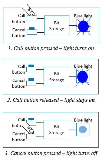
Flight Attendant Call Button System
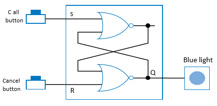
Cross-Coupled NOR SR Latch Schematic
Operational Analysis & States
| Inputs () | State | Output () | Complement () | Description |
|---|---|---|---|---|
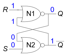
| Set | Forces output to . | |||
| Reset | Forces output to . | |||
| Hold / Memory | Retains previously stored state. | |||
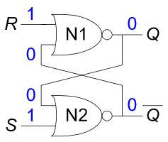
| Invalid / Forbidden | Illegal State: Violates . |
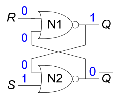
Set State Operation ()
Reset State Operation ()
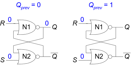
Hold Memory State Operation ()
Invalid Forbidden State ()
Hazard of the Invalid State ( )
If and are simultaneously active () and then simultaneously released to , the final state of becomes unpredictable due to non-deterministic propagation delays along asymmetric feedback paths, causing output oscillation or settling into an unintended state (metastability).
Characteristic Equation & State Diagram
Breaking the feedback loop () yields the next-state truth table and K-Map derivation:
| Function | ||||
|---|---|---|---|---|
| Hold () | ||||
| Hold () | ||||
| Reset () | ||||
| Reset () | ||||
| Set () | ||||
| Set () | ||||
| Forbidden / Disallowed | ||||
| Forbidden / Disallowed |
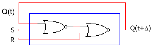
Feedback Path Interruption for Characteristic Derivation
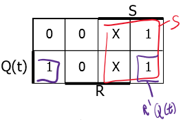
K-Map for Next-State
Characteristic Equation
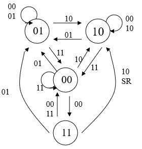
SR Latch State Transition Diagram
Level-Sensitive Gated SR Latch & Clocking
Adding a control/enable signal ( or ) prevents inputs from changing state uncontrollably.
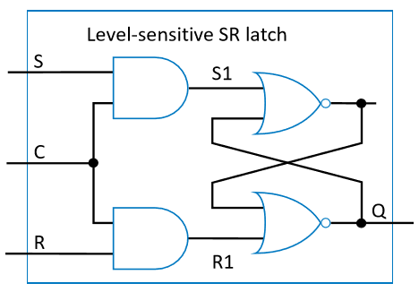
Gated / Level-Sensitive SR Latch
- When : and . The latch is forced into Hold Mode regardless of and inputs.
- When : External and inputs pass through to drive the internal SR latch.
Risk Reduction
Adding an enable control signal reduces the probability of an invalid condition occurring by restricting state updates strictly to times when inputs are known to be stable.
Clock Signal Metrics
Sequential logic circuits use periodic clock signals to synchronize data transfers across latches and flip-flops.
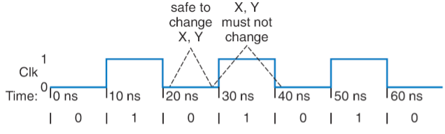
Periodic Clock Waveform and Parameter Definitions
- Clock Period (): Total duration of one complete clock cycle (e.g., ).
- Clock Frequency (): Number of cycles per second:
- Duty Cycle: The ratio of time the clock is HIGH during one period:
Level-Sensitive D Latch
The D Latch (Data Latch) eliminates the invalid state by placing an inverter between the and inputs.
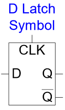
D Latch Block Symbol
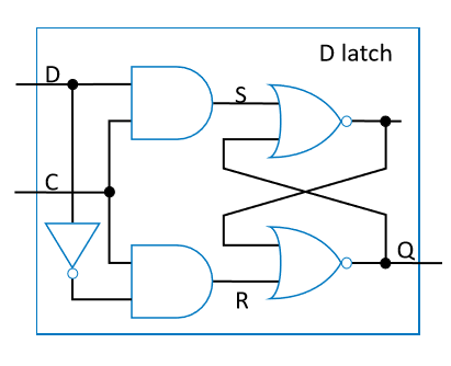
Gated D Latch Circuit Schematic using an Inverter
Operational Summary
- When (Transparent Mode): Inputs set and . The input passes directly to output .
- When (Opaque / Hold Mode): Internal signals drop to . Output holds its previous value.
Transistor-Level Complexity Breakdown
Constructing a standard gated D latch from CMOS gates requires 22 transistors ():
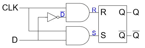
Transistor-Level Diagram of Static CMOS D Latch
D Latch Truth Table
| Internal | Internal | Operational State | |||||
|---|---|---|---|---|---|---|---|
| Hold (Opaque) | |||||||
| Reset () | |||||||
| Set () |
D Flip-Flop (Master-Slave Edge-Triggered Storage)
Level-sensitive latches remain transparent as long as , allowing data to propagate through multiple cascaded latches within a single clock cycle (race condition). A D Flip-Flop solves this by sampling input strictly on a clock transition (edge).
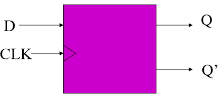
Edge-Triggered D Flip-Flop Symbol
Master-Slave Architecture
A Master-Slave D Flip-Flop connects two D latches in series driven by inverted clock signals:
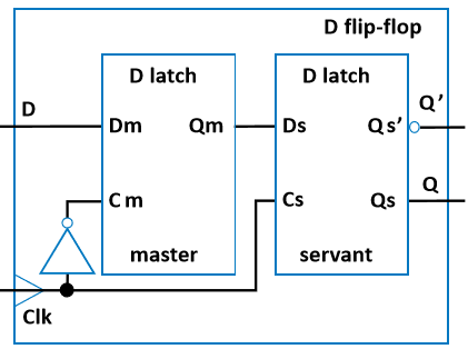
Master-Slave D Flip-Flop Internal Architecture
- Phase 1 ():
- Master Latch (): Transparent. is sampled into internal node .
- Slave Latch (): Opaque (Hold). Output maintains previous state.
- Phase 2 ( Transition / Rising Edge):
- Master Latch (): Becomes opaque, isolating from input changes.
- Slave Latch (): Becomes transparent, passing captured node directly to final output .
Characteristic Equation
Rising Edge vs. Falling Edge Comparison
| Feature | Rising Edge D Flip-Flop | Falling Edge D Flip-Flop |
|---|---|---|
| Symbol | 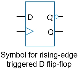 | 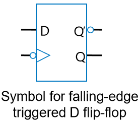 |
| Inverter Placement | Inverter drives Master Clock () | Inverter drives Slave Clock () |
| Active Edge | Transition | Transition |
| Timing Waveform | 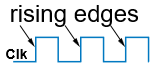 | 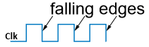 |
Enhanced D Flip-Flop Features
Enabled D Flip-Flop (Load Enable / )
Instead of gating the clock line (which introduces clock skew), an Enabled D Flip-Flop uses an input multiplexer controlled by to loop the output back when disabled:
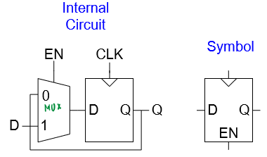
Enabled D Flip-Flop using Feedback Multiplexer
- When : Multiplexer selects new input . updates on active clock edge.
- When : Multiplexer selects current . retains state across cycles.
Reset and Preset Controls
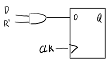
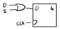
Flip-flops include controls to force the initial state to (Reset ) or (Set/Preset ).
Reset (set state to 0) ―
- synchronous: (when next clock edge arrives)
- asynchronous: doesn’t wait for clock (inside FF)
Preset or set (set state to 1) ― S (sometimes P)
- synchronous: (when next clock edge arrives)
- asynchronous: doesn’t wait for clock (inside FF)
Both reset and preset
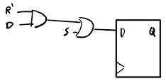
Synchronous Control
Updates occur only on the active clock edge. The control signal is gated into the data input :
Asynchronous Control
Overrides the clock line and updates state immediately via direct clear/preset lines in the internal latches.
Priority Dominance Equations
Evolution of Bit Storage Elements
| Memory Element | Key Feature | Primary Disadvantage |
|---|---|---|
SR Latch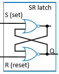 | Cross-coupled NOR feedback. Simple set, reset. | creates invalid/forbidden output state. |
Gated SR Latch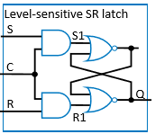 | Added enable signal . Limits update window. | Must guarantee never occurs while . |
D Latch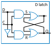 | Single data input . Eliminates state. | Level-sensitive: Remains transparent as long as . |
D Flip-Flop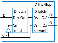 | Edge-triggered Master-Slave design. Samples only on edge. | Larger internal gate count than basic latches. |
Latch vs. Flip-Flop Waveform Comparison
The timing diagram below illustrates the fundamental operational difference between a Level-Sensitive D Latch and a Positive Edge-Triggered D Flip-Flop:
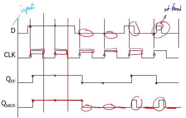
Timing Comparison between D Latch and Positive Edge-Triggered D Flip-Flop
- D Latch Output (): Continuously tracks input whenever (transparent window).
- D Flip-Flop Output (): Captures the value of only at the exact moment transitions from and holds it stable for the rest of the cycle.