Abstract
Memory modules are classified across ROM (Read-Only Memory), RAM (Random-Access Memory), and NVM (Non-Volatile Memory). This note details array organization, memory expansion composition methods (widen words and deepen address spaces), square matrix topology, and physical cell mechanics across Register Files (), Static RAM (), and Dynamic RAM ().
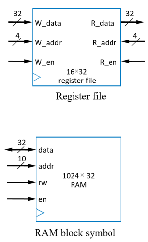
Array Organization & Signal Interface
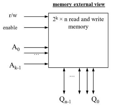
A memory module of dimensions stores addressable words of bits each.
- Words: Total addressable memory locations ().
- Address Lines: Calculated via .
- Data Lines: Multi-bit word width ().
- Control Lines: Read/Write () and Enable ( / Chip Select).
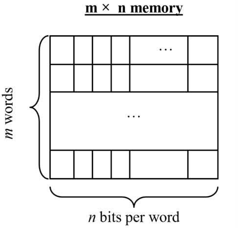
Memory Module
- Capacity: ().
- Address Lines (): .
- Data Bus (): .
Memory Composition Techniques
1. Wider Words (Bit-Width Expansion)
To widen word size () while maintaining word count ():
- Connect memory modules side-by-side.
- Connect address () and control (, ) lines in parallel.
- Concatenate data lines to form a wider multi-bit bus ().
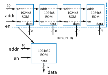
Word Widening ()
More Words (Address-Space Expansion)
To increase total addressable words () while maintaining word width ():
- Stack memory modules vertically.
- Drive lower address bits () to all chips in parallel.
- Use upper address bit(s) to drive a decoder asserting the target chip’s Enable line ().
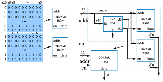
Address Expansion ()
Physical Storage Cell Comparison (RAM Spectrum)
| Property | Register File (FF) | Static RAM (SRAM) | Dynamic RAM (DRAM) |
|---|---|---|---|
| Transistor Count / Cell | (Multi-port D-FF) | (1 Transistor, 1 Capacitor) | |
| Access Latency | (+ Refresh overhead) | ||
| Density & Area | Lowest density / Largest area | Compact | Extremely Compact / Highest Density |
| Volatility | Volatile | Volatile | Volatile (Requires periodic refresh) |
| Diagram | 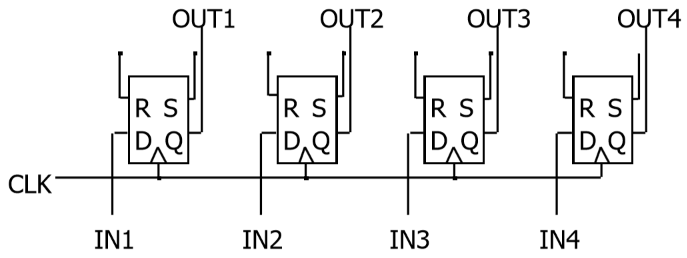 | 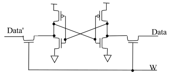 | 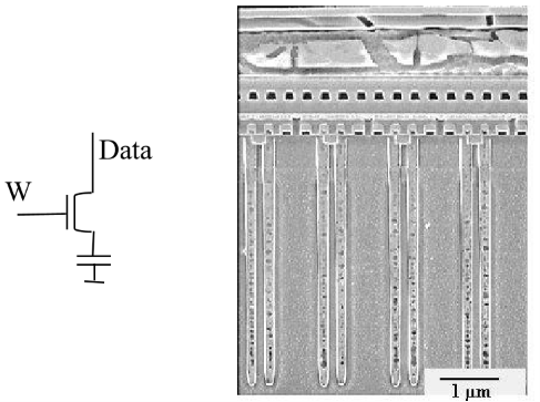 |
RAM Internal Architecture & Cell Operations
RAM arrays are laid out in a square matrix grid to balance row (word line) and column (bit line) capacitance.
Logically the same as register file, but RAM has only 1 port; register file has two or more
RAM vs. Register File
RAM is larger, stores more bits using a bit storage vs. FFs, and implemented on a chip in a square ― keeps longest wires (hence delay) short
RAM Internal Structure
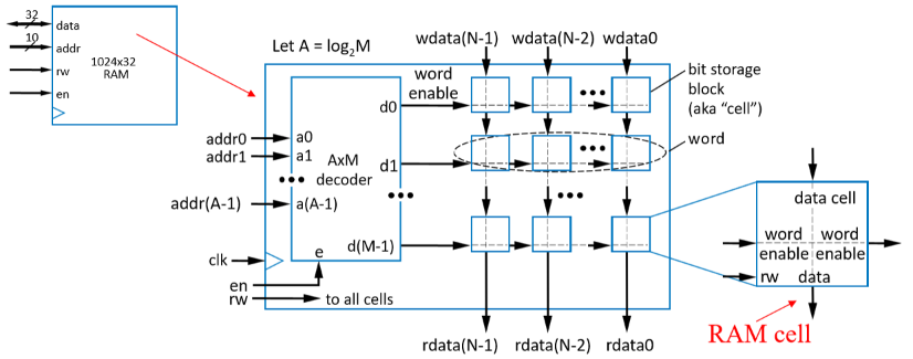
Square Array Grid and Internal Decoder Layout
Similar internal structure as register file
- Decoder enables appropriate word based on address inputs
- controls whether cell is written or read
- Let’s see what’s inside each RAM cell
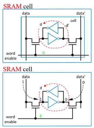
SRAM 6T Mechanics:
Uses two cross-coupled inverters and two access transistors.
Write
- word enable input comes from decoder
- When , value loops around inverters ― storing the bit
- When , the data bit value enters the loop
- data is the bit to be stored in this cell
- data’ enters on the other side
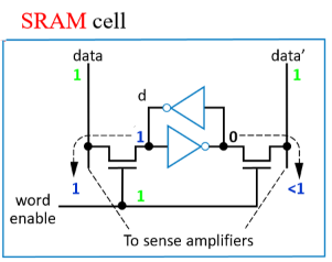
Read
- When set to read, the RAM logic sets both data and data’ to
- The stored but will pull either the left bit or right bit down slightly below
- Evaluated by Sense Amplifiers which detects which side is slightly pulled down by sensing voltage difference
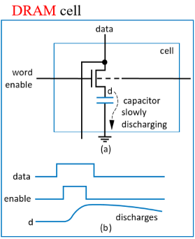
DRAM 1T1C Mechanics:
Stores charge on a large capacitor via a single pass transistor. Because charge leaks off over time, DRAM requires periodic refresh cycles (typically every ).
- write: transistor conducts, data voltage level gets stored on top plate of capacitor
- read: just look at value of