Abstract
Electronic switches serve as the physical foundation of modern binary digital systems. CMOS (Complementary Metal-Oxide-Semiconductor) technology combines nMOS transistors (which form Pull-Down Networks connected to ground) and pMOS transistors (which form Pull-Up Networks connected to supply voltage ). By combining nMOS and pMOS in parallel, Transmission Gates act as ideal bilateral switches that avoid voltage degradation. Transistor-level implementations of NAND and NOR gates demonstrate functional universality, enabling all Boolean logic functions to be synthesized from basic switch networks.
Electrical Terminology & Physical Foundations
Digital logic signals are physical voltage levels. Analyzing gate delays and dynamic power consumption requires understanding key electrical parameters:
- Voltage (): The difference in electrical potential between two points, measured in Volts. Represents digital logic states ( for Logic 1, Ground/GND for Logic 0).
- Current (): The flow rate of charged particles through a conductor, measured in Amperes.
- Resistance (): The tendency of a material or wire to impede current flow, measured in Ohms ().
- Capacitance (): The ratio of electric charge change to electric potential change, measured in Farads (). Gate terminals and interconnect wires behave as parasitic capacitors.
Physical Switching Behavior
Charging a capacitance to voltage requires finite time . This charging/discharging current limits the maximum operating clock frequency of digital circuits.
CMOS Switch Fundamentals
CMOS (Complementary Metal-Oxide-Semiconductor) technology uses paired n-channel (nMOS) and p-channel (pMOS) field-effect transistors to construct digital logic with near-zero static power dissipation.
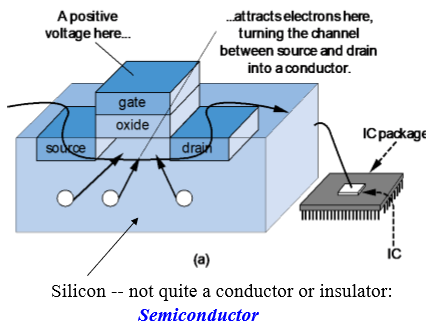
CMOS Complementary Transistor Pair Structure
nMOS vs. pMOS Transistors
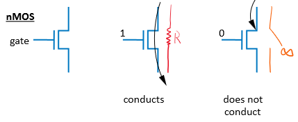
nMOS Transistor Switch
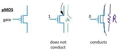
pMOS Transistor Switch
| Property | nMOS Transistor | pMOS Transistor |
|---|---|---|
| Active Control Input | Logic 1 ( / positive charge) | Logic 0 ( / negative charge) |
| Switch State when Gate = 1 | ON (Closed Circuit) | OFF (Open Circuit) |
| Switch State when Gate = 0 | OFF (Open Circuit) | ON (Closed Circuit) |
| Strong Signal Transmission | Passes 0 well (Strong ) | Passes 1 well (Strong ) |
| Weak Signal Transmission | Passes 1 poorly () | Passes 0 poorly () |
| Network Configuration | Pull-Down Network (PDN) | Pull-Up Network (PUN) |
| Rail Connection | Connected to Ground () | Connected to Power () |
Transistor Circuit Design: PUN and PDN
A static CMOS gate consists of two complementary networks operating mutually exclusively:
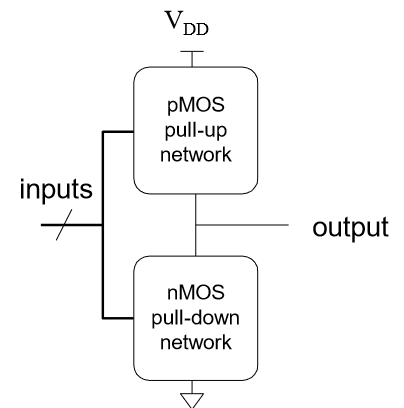
Static CMOS Dual Network Structure (Pull-Up and Pull-Down Networks)
- Pull-Up Network (PUN): Composed exclusively of pMOS transistors connected between and the output node. When active, it pulls the output to a strong Logic 1.
- Pull-Down Network (PDN): Composed exclusively of nMOS transistors connected between the output node and . When active, it pulls the output to a strong Logic 0.
Dual Network Rule
For any valid input combination, either the PUN connects the output to or the PDN connects the output to . They are never ON simultaneously (which would cause a short circuit) nor both OFF simultaneously (which would leave the output floating).
Transmission (Pass) Gates
Using a single transistor type as a switch introduces signal degradation:
- An nMOS switch alone passes s strongly, but degrades s.
- A pMOS switch alone passes s strongly, but degrades s.
A Transmission Gate (TG) combines an nMOS and a pMOS transistor in parallel to create a full-rail bilateral switch.
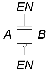
Transmission Gate Circuit Schematic and Symbol
Operational States
- Enabled (): Both transistors turn ON. Input connects directly to output . The nMOS strongly passes low voltage (), while the pMOS strongly passes high voltage ().
- Disabled (): Both transistors turn OFF. Input is disconnected from . The output node enters a High-Impedance state ( / sleep mode).
| Enable () | Complement () | nMOS State | pMOS State | Output () |
|---|---|---|---|---|
| OFF | OFF | High-Impedance () | ||
| ON | ON | Connected to Input () |
Transistor-Level Gate Implementations & Universality
Any Boolean function can be constructed using only NAND gates or only NOR gates (Functional Universality).
Universal Logic: NAND Implementations
A basic 2-input NAND gate consists of 4 transistors: 2 pMOS in parallel (PUN) and 2 nMOS in series (PDN).
1. NOT Gate (Inverter)
Constructed by wiring a 2-input NAND gate with inputs tied together (or using a standard 2-transistor CMOS inverter):
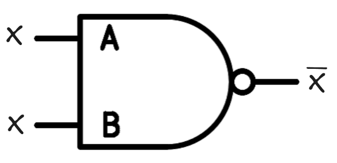
NAND-configured NOT Gate (4 Transistors)
- Transistor Count: 4 Transistors (when using a 2-input NAND) / 2 Transistors (standard CMOS Inverter).
2. AND Gate
Constructed by cascading a 2-input NAND gate with an Inverter:
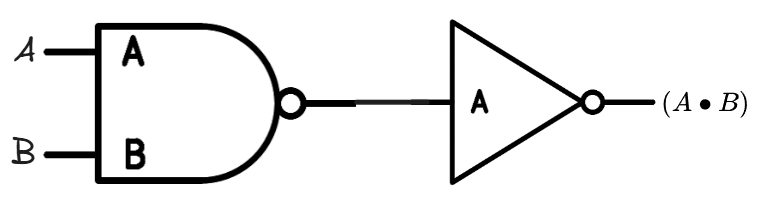
NAND-based AND Gate
- Transistor Count: 6 Transistors ().
3. OR Gate
Constructed using De Morgan’s Law () by inverting inputs before feeding a NAND gate:
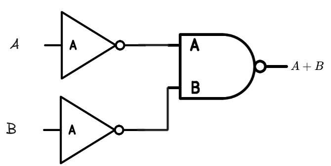
NAND-based OR Gate Structure
- Transistor Count: 8 Transistors ().
Universal Logic: NOR Implementations
A basic 2-input NOR gate consists of 4 transistors: 2 pMOS in series (PUN) and 2 nMOS in parallel (PDN).
1. NOT Gate (Inverter)
Constructed by tying the inputs of a 2-input NOR gate together:
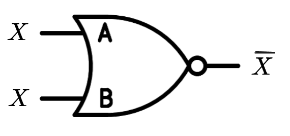
NOR-configured NOT Gate (4 Transistors)
- Transistor Count: 4 Transistors (when using a 2-input NOR).
2. OR Gate
Constructed by cascading a 2-input NOR gate with an Inverter:
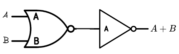
NOR-based OR Gate
- Transistor Count: 6 Transistors ().
3. AND Gate
Constructed using De Morgan’s Law () by inverting inputs before feeding a NOR gate:
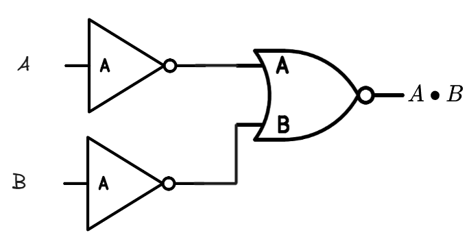
NOR-based AND Gate Structure
- Transistor Count: 8 Transistors ().
Summary of Gate Transistor Counts
| Desired Logic Gate | NAND-Based Construction | NOR-Based Construction | Total Transistor Count |
|---|---|---|---|
| NOT | NAND with inputs tied | NOR with inputs tied | 4 (or 2 for standalone Inverter) |
| AND | NAND + NOT | NOTs + NOR | 6 (via NAND) / 8 (via NOR) |
| OR | NOTs + NAND | NOR + NOT | 8 (via NAND) / 6 (via NOR) |