Abstract
Timing Analysis in digital circuits guarantees that logic signals propagate cleanly without violating storage element setup and hold constraints. Because real-world logic gates and wires experience physical electrical delays (), signals do not change instantaneously. Combinational timing is bounded by contamination delay () and propagation delay (). In sequential circuits, registers impose strict setup () and hold () time windows relative to clock edges. Additionally, spatial variation in clock signal arrival—known as Clock Skew ()—degrades the maximum operating frequency () and increases the risk of hold time race conditions.
Combinational Logic Timing Dynamics
Signals flowing through combinational networks experience delays dictated by transistor capacitance and resistance ().
flowchart LR
    T0["<b>t = 0</b><br>Input Change"] -->|"Output Unstable"| TCD["<b>t = t_cd</b><br>Contamination Delay"]
    TCD -->|"Output Settling"| TPD["<b>t = t_pd</b><br>Propagation Delay"]
    TPD --> STABLE["<b>Output Guaranteed Stable</b>"]
- Contamination Delay (): The minimum time from when an input changes until the output starts to change. It is determined by the shortest delay path (fewest gates) through the circuit:
- Propagation Delay (): The maximum time from when an input changes until the output is guaranteed to reach its final stable value (stops changing). It is determined by the critical path (longest delay path) through the circuit:
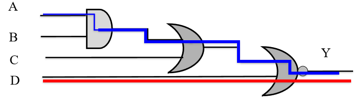
Shortest Path (Red / ) vs. Critical Path (Blue / ) in Combinational Logic
Sequential Timing Parameters
Flip-flops require inputs to remain stable around the active clock edge to reliably capture state without entering a metastable condition.
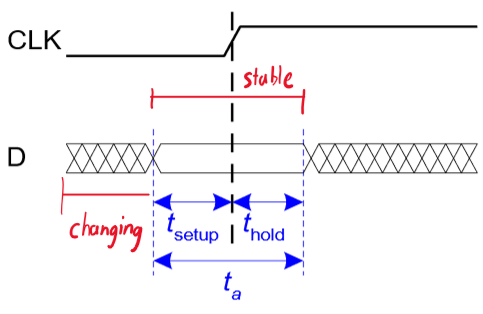
Sequential Timing Windows around Active Clock Edge
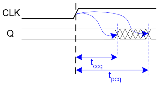
Flip-Flop Output Delay Ranges ( and )
Storage Element Constraints
- Setup Time (): Minimum duration before the active clock edge that data input must remain completely stable.
- Hold Time (): Minimum duration after the active clock edge that data input must remain completely stable.
- Aperture Time (): Total window around the clock edge during which data must not change:
Clock-to-Q Output Delays
- Clock-to-Q Contamination Delay (): Minimum time after the clock edge before output begins to change (might become unstable).
- Clock-to-Q Propagation Delay (): Maximum time after the clock edge when output is guaranteed to be stable at its new value.
Ideal Clock Timing Constraints
In an ideal system where the clock edge arrives at all flip-flops simultaneously, the clock period and combinational paths must satisfy two critical constraints:
flowchart LR
    Reg1["<b>Register 1</b>"] -->|"t<sub>pcq</sub> / t<sub>ccq</sub>"| Logic["<b>Combinational Logic</b>"]
    Logic -->|"t<sub>pd</sub> / t<sub>cd</sub>"| Reg2["<b>Register 2</b>"]
Setup Time Constraint (Max Delay Limit)
The total delay along the longest path between two registers must be shorter than one clock cycle () minus the setup time required by the destination flip-flop.
Fixing Setup Violations
A setup violation means the data path is too slow (or clock frequency is too high). It can be resolved by:
- Increasing the clock period (lowering operating frequency).
- Pipelining or reducing the critical path logic delay ().
Hold Time Constraint (Min Delay Limit)
The fastest possible signal update from the launching register must not arrive at the destination register before its hold time window has elapsed.
Fixing Hold Violations
A hold violation means the data path is too fast—the new value overwrites the old value before the destination register finishes sampling. Lowering the clock frequency cannot fix a hold violation because hold constraints are independent of .
Fix: Insert intentional delay along the minimum delay path (e.g., adding two NOT gates / buffers in series).
4. Clock Skew Analysis ()
In real physical chips, wire interconnect lengths and buffer delays cause the active clock edge to arrive at different registers at slightly different times. The maximum arrival time difference between any two registers is defined as Clock Skew ().
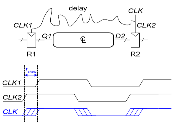
Clock Skew between Launching Register (CLK1) and Receiving Register (CLK2)
Setup Time Constraint with Clock Skew
Worst-Case Scenario: arrives earlier than by (destination clock is early), shrinking the available clock cycle time.
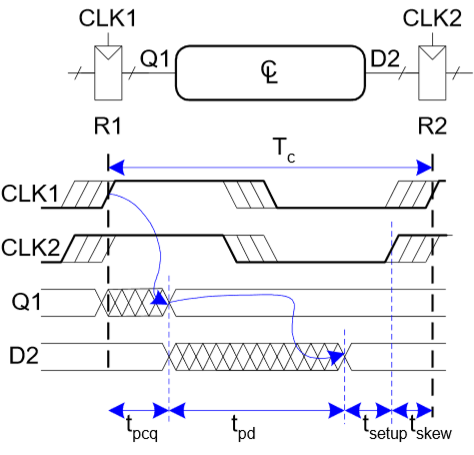
Setup Timing Analysis under Worst-Case Early Receiving Clock ()
Hold Time Constraint with Clock Skew
Worst-Case Scenario: arrives later than by (destination clock is delayed), giving the launching register extra time to prematurely overwrite the receiving register’s input.
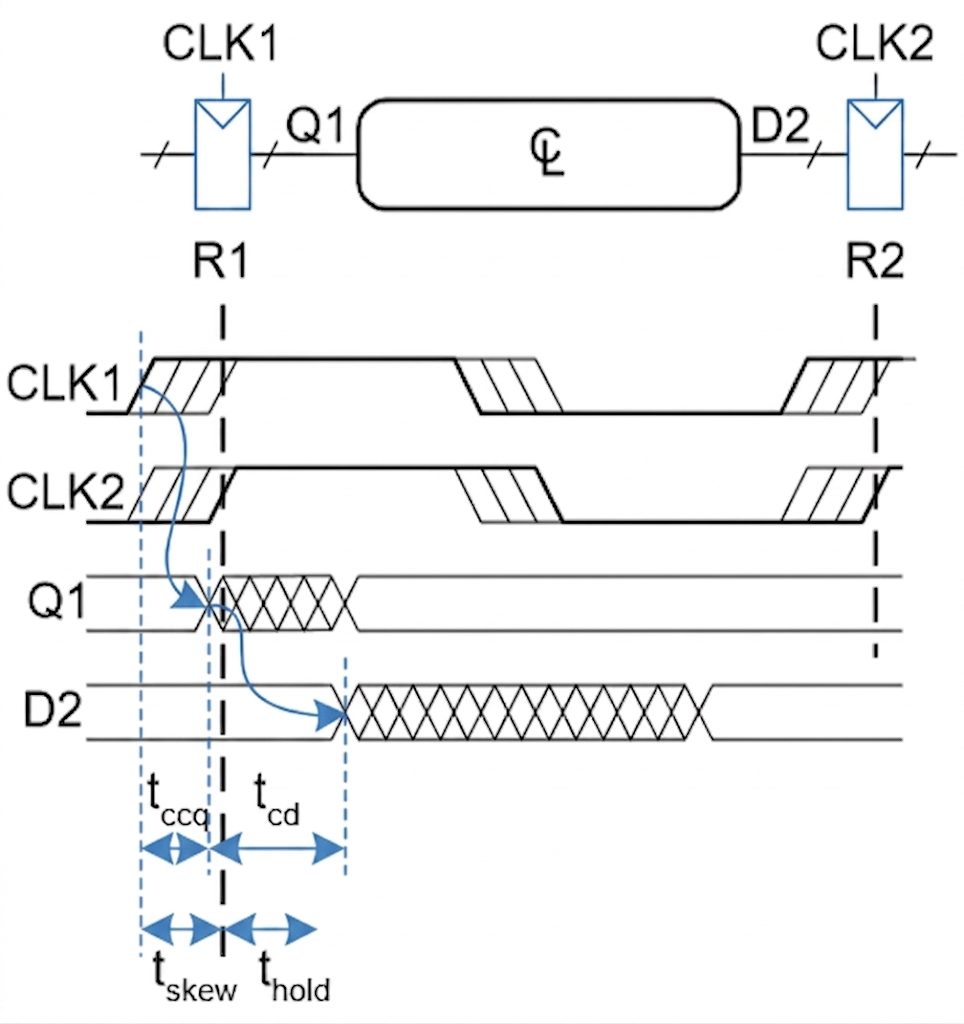
Hold Timing Analysis under Worst-Case Late Receiving Clock ()
Constraint Summary Reference
| Constraint | Ideal Clock Equation | Equation with Clock Skew () | Primary Impact |
|---|---|---|---|
| Setup Time (Max Delay) | Determines maximum clock frequency () | ||
| Hold Time (Min Delay) | Guarantees data integrity (independent of ) |